Printed Circuit Board (PCB) Layout
AirBorn does offer PCB layout as a seperate service, but more often it is as part of the whole Custom electronics PCB design project - where the client wants the circuit, CAD and prototyping stages as well. Please Email
PCB Layout software
AirBorn supports thhe Protel PCB layout package. This is an older package that is Freeware from Protel and runs in the current windows environment under DosBox.
PCB etching (The Laminate)
AirBorn subcontracts etching - we describe the base PCB laminate etching processing on a seperate page - should we link to manufacturers? Email
PCB Assembly
AirBorn subcontracts most PCB assembly, again we have a seperate page. We go into a lot of detail about selecting PCB assembly subcontractors.
The Whole Design Method
This is what AirBorn does: The whole design process, the page you are currently on is the third or fourth of about 12 describing the steps. The series started here

The connections on a PCB should be identical to its corresponding circuit diagram, but while the circuit diagram is arranged to be readable, the PCB layout is arranged to be functional, so there is rarely any visible correlation.
PCB layout can be performed manually (using CAD) or in combination with an Autorouter. The best results are usually still achieved using atleast some manual routing - simply because the design engineer has a far better judgement of how to arrange circuitry. Surprisingly, many autorouted boards are often completely illogical in their track routing - the program has optimised the connections, and sacrificed any small amount of order that may have been put in place by manual routing. Generally autorouted boards are somewhat harder for a technician to repair or debug, for this reason. Historically, PCBs used to be laid out by using stick on paper shapes and tape on mylar drafting film, - that really WAS manual routing!
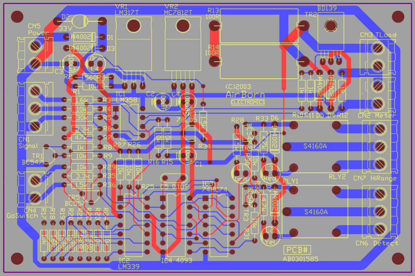
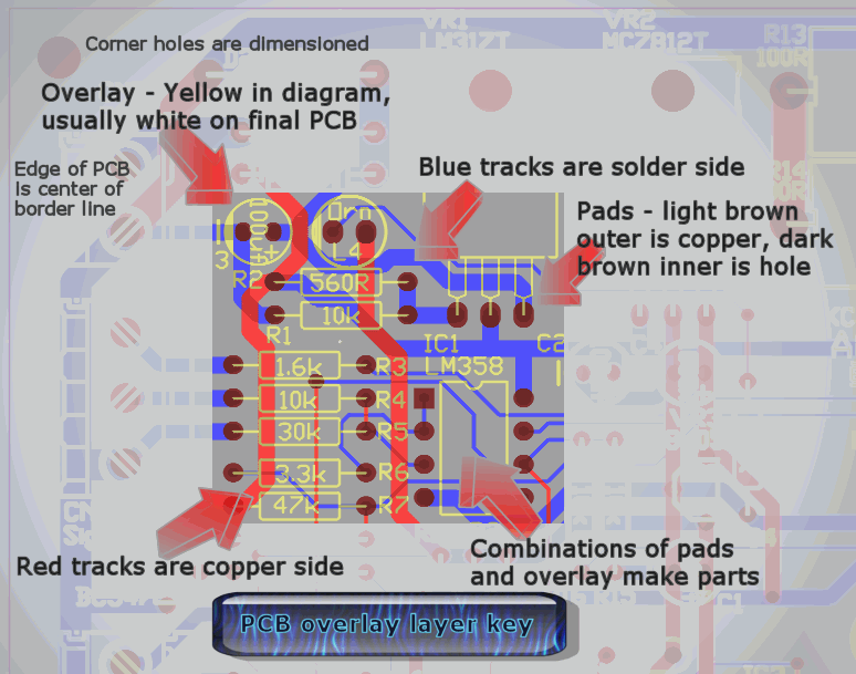
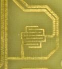
The CAD PCB layout consists of several layers, for illustration often the layers will be coloured and compressed into the one overlay image. (Click here to see a typical overlay, and Click here to see a colour coded key diagram) The circuit design and the PCB overlay image will usually be supplied by the designer to the client in a PDF document produced by the CAD package. The PCB overlay may quite easily be printed out actual size, cut out, and used for approximate size comparisons with mechanical items - for instance the print can be placed inside the actual enclosure, to see how it will be positioned in relation to other parts. Components can also be placed up against the pad markings as a quick idiot-check of dimensions.
It is worth putting a bit of effort into the PCB design - it is somewhere where quality of design can make a difference. The width of the tracks is a trade-off based on current flow, space available, size of parts, and electromagnetic interference. The track layout is a similar trade-off that also picks when to dodge from one side of the board to the other to avoid an obstacle, but overall normally aims to find the shortest regular path between the connected points. Given the impedance, susceptibility, and signal on tracks, the loop area is another trade-off that is considered as the design proceeds. And then, added to all that is Design-for-manufacture.
 A rotten layout |
 A better replacement |
These days most circuit boards are automatically assembled and tested -
but people still install and repair them.
![]() Having a quality design can make all the difference between a product that is pleasant to work
on and one that they will hate. Machine test points, for ATE (Automated Test Equipment) bed of
nails testing, only need to be plain pads or lands. Some test points, however, are really intended
to be for engineering test or modification - for these it is better to put in labelled, circled
pads.
Having a quality design can make all the difference between a product that is pleasant to work
on and one that they will hate. Machine test points, for ATE (Automated Test Equipment) bed of
nails testing, only need to be plain pads or lands. Some test points, however, are really intended
to be for engineering test or modification - for these it is better to put in labelled, circled
pads.
Most PCBs have a silkscreen identification overlay (usually white on Green PCBs). Improving the overlay is another way to make a better PCB. The silkscreen contains important information that assists people to build, service and install the product. Aside from the PCB functionality (which is rather obvious) the overlay is the chief distinguishing feature between a purpose-built product, and a general-purpose controller or ready made PLC. A well made custom or purpose-built product would label terminals as: "+12v red" "-pwr black" "solenoid+" "solenoid-" whereas a general purpose kit board may often just give you: "A1 A2 A3 A4". The makers of the kit board don't have much of a choice - they have no idea what you will attach to the terminals.
As PCB component density rises, it is often necessary to reduce the labelling - there is just not enough room. The first best measure is to drop the size of the lettering. Then either move the component values under components (where they may possibly be read before board assembly, and definitely still read in the documentation overlay diagram) or omit the values. Then last do the same, if absolutely needed, for the designators. The pin 1 labelling and orientation labelling for components and connectors cannot be removed - even when automated pick and place machines are used, the visual backup is imperative for assembly and repair.
The silkscreen is the primary method for labelling connectors, replaceable parts, orientation, and even installation notes (for instance "Remove J2 while replacing battery - observe battery polarity"). It can also used as a backup for manufacturing notes (for example "Mount R2 approx 5mm off circuit board due to high temperature", or more likely "Space up 5mm: HOT") although now it is probably more usual to put these notes in the BOM. With the way the electronics industry is changing at present, there are more third-party boards with a substantial amount of Chinese language labelling on the Silkscreen. It certainly makes those boards more difficult (for us) to use.
The PCB layout also needs to take account of electrical interference. The main techniques used are shielding using areas of copper, and reduced power supply impedance using either multilayer boards (the best, although more expensive, solution) or increased width of power supply tracks. There is further information on this EMI and ESD compliance page. AirBorn has an (older) tutorial on designing PCBs - it steps through the CAD process from schematic to layout. AirBorn Electronics supports the (free) Autotrax CAD package. For those intending to design PCBs themselves, we recommend this manual on PCB layout.
The truth is rarely pure, and never simple. -- Oscar Wilde
Most standard Etched PCB laminates are:
- Double sided Laminate
- Two layers of copper tracks, one each side of the board
- In progressively smaller Quantities
- 4 Layer, 6 Layer, 8 Layer
The real advantage with 4 layer boards is that the internal layers are usually dedicated power distribution - this decreases the loop area and power supply impedance giving a dramatic boost to EMI performance. 6 layers and above adds extra layers for PCB tracks, allowing denser higher performance circuitry. As a very rough rule of thumb, PCBs are often priced "per layer" - ie the bare laminate for an 8 layer board may perhaps be 4 times the price of its 2 layer equivalent. - Plated Through Hole
- PTH - each hole is copper plated providing a circuit between sides of the PCB. Normally AirBorn also Tent the vias - cover them with solder mask - others may do this or leave the soldermask open over vias so that they fill up when wave soldered.
- Fibreglass-resin laminate (FR4) is the standard dielectric material.
- Solder Mask Over Bare Copper
- SMOBC - green insulating ink everywhere except connections (Other colours are available - commonly White, Black, Blue, Red)
- Component legend
- Identifying lettering, component outlines and values (usually) in white ink
- Immersion Silver for ROHS compliant work (a definition for ROHS is further below)
- Silver plate on all exposed copper, prevents oxidation and so keeps the surface solderable. An alternative is electroless gold.
- Tinned For non-ROHS work
- Tinning is application of Lead-Tim Solder to all exposed copper, increasing solderability
- Hot Air Solder Levelled: HASL
- Hot oil - or hot air (HASL) - levelling makes the tinning flat, so that surface mount components can be positioned reliably.
Different methods of PCB construction:
- Conventional
- A rigid PCB (usually of thickness 1.6mm), with wire-leaded components mounted on only one side of the PCB, with all the leads through holes, soldered and clipped. Conventional circuitry is generally easier to debug and repair than Surface mount.
- Surface Mount Technology (SMT) or devices (SMD)

- A PCB with tag-leaded components soldered flush to PCB pads. Holes are still needed on the PCB, but not where the component leads are attached. Surface mount circuitry is generally smaller than conventional. Surface mount is generally more suited to automated assembly than conventional.
- Surface mount & conventional mix
- In practice, most boards are a mix of surface mount and conventional components. This can have its disadvantages as the two technologies require different methods of insertion and soldering.
- Double sided Laminate
- A bare PCB laminate having tracks on both sides, normally with PTH holes connecting circuitry on the two sides together.
- Double sided Component Assembly
- Mounting components on both sides of the PCB. Normally only surface mount circuitry would be mounted on both sides of a PCB, but some conventional components (such as LEDs) may be mounted on the reverse of a PCB to suit the enclosure design.
- Multi-layer
- A PCB Laminate may be manufactured with more than two layers of copper tracks by using a sandwich construction. The cost of the laminate reflects the number of layers. The extra layers may be used to route more complicated circuitry, and/or distribute the power supply more effectively.
- Gold plated
- Certain areas on a PCB may be gold plated for use as contact pads or as a ROHS-compliant board finish. Normally only a thin gold plating is required, and this can be achieved with electroless gold. If a thicker gold plating is required (for instance a quality 50um contact) an electrolytic process is needed. Normally this is limited to pads on the edge of a PCB, as an electrolytic plating bar must be attached to the pads, and then removed part way through the PCB manufacturing process. Gold plating normally needs a nickel underplate or the Gold quickly disappears through migration effects into the underlying copper.
- Immersion Silver plating
- A ROHS-compliant board finish that is a cost effective alternative to Gold
- ROHS Compliance
- Simple definition: Getting rid of the Lead in PCBs and components which poisons groundwater when it leaches out of discarded boards put in landfill waste dumps. Actually, lead is not the only substance covered, but it is the main one. Frankly it would also help if people stopped throwing away so much electronics, and that would be helped if boards were made to last.
- Flexible PCB
- A technique used extensively with membrane keyboards, combination connector/circuit boards, and circuit boards to fit in awkward shapes - e.g. cameras.
- Chip On Board (COB)
- Where the IC die is attached direct to a PCB, and bond out wires from the IC connect directly to PCB lands. The chip is then covered with a black blob of epoxy. A technique used mostly with very high volume, cost sensitive applications, e.g. musical greeting cards, LCD modules, calculators, some toys.
- Phenolic PCB
- As distinct from Fibreglass, Phenolic is a cheaper PCB laminate material.
- Single sided Laminate
- Most PCB laminates produced these days are double sided - wtih tracks on both sides of the board, and PTH vias joining the two sides. An alternative, most usually used with Phenolic PCBs, is single sided: Tracks on just one side. A limited number of connections are usually still needed on the top side of the board, and these are made with wire links. Single sided boards are cheaper to manufacture as no plating line is needed, and copper is only required on one face of the laminate, halving the resist and exposure work. However, in todays market, the price difference between single and double sided is not that great. The savings are realistic only for huge runs of relatively unsophisticated consumer electronics, such as pocket calculators.
- Daughterboard
- A circuit board mounted to another circuit board - such as a plug in card.
Reality is merely an illusion, albeit a very persistent one
-- Albert Einstein ![]()
- Contact Us
- Enquiry Form
- Sitemap
- The PCB design method
- About Circuit diagrams
- About PCB layout
- About Firmware design
- Spec'ing your job
- Our design service
- Example Projects Library
- Mechatronic control unit
- Garbage truck compactor
- RS232-RS485 convert (2006)
- Tone generator test project
- RS485 fire panel int.
- Front panel switches( A/D)
- Serial to IRDA
- Danfoss loop tester
- RAN Multilayer trainer
- Programmable Oscillator
- Pressure sense PCB
- Nursecall overdoor light V2
- Design step-by-step
- Circuit diagrams
- PCB Layout
- PCB Etching
- Prototyping
- Firmware design
- Documentation
- Manufacturing
- Economies of scale
- Test Procedures
- ECOs - changes
- EMI & ESD in design
- FR4 and fire resistance
- Project Specifications
- Specification Intro.
- Writing a Spec
- Tech Ingredients
- Example Specs (older)
- Selecting a designer
- R&D Economics
- Design Inspiration
- Autotrax Utitilities
- Autotrax links
- Our PicoBus IO Std
- RS232 connectors
- Our RS485 converter
- P89LPC932
- Our Program header
- How to use a Multimeter
- Our Site index
- Offsite Links (15000+)
- Google search
- Contact
©2013 AirBorn - Last updated 01 May 2013