The Printed Circuit Board (PCB) Layout --- A Tutorial
This project demonstrates how to produce an electronic project using one particular PCB CAD package: Autotrax. The PCB design process is an important part of producing finished custom electronics. This page goes through circuit design, PCB design, shows the prototype, an error is found, and then the design is repaired. An Error or three is par-for-the-course when building new designs - that is why we build prototypes.
This page could help new designers wanting to learn principles, and is ideal for Autotrax users as a tutorial. The page may also be useful to people who project manage the electronics design process - but realistically, if you are not hands-on-tools you will probably find the information presented to be just a little too detailed.
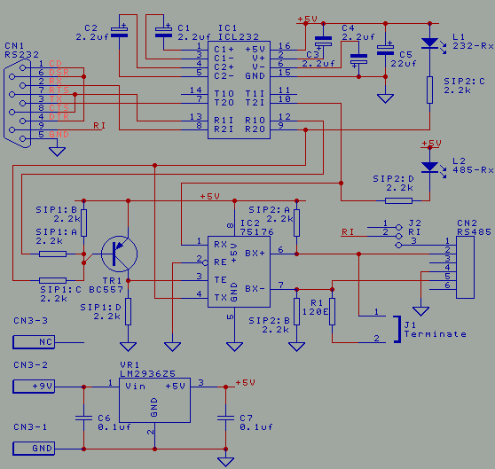
This project is an RS232 to RS485 converter. The circuit demonstrates a lot of principles of circuit design, and hopefully the finished project is useful.
First, the specification - to do things "by the book" - this defines goals and sets limits.
RS232 to RS485 Converter specification
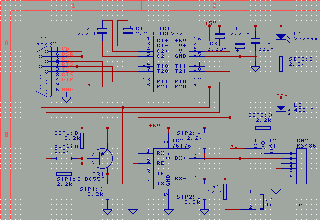
As the design proceeded we added a couple of extra features over and above the specification, for the sake of completeness we add them back here now:
|
By using a Schematic CAD Package to create the circuit diagram, then generating a Netlist to use as the input to a PCB CAD package, the designer has the benefit of being able to run a Design Rule Check to verify that the final PCB matches the original circuit.
Most engineers choose to start the circuit design on paper. Some designers, especially when starting out and attempting their first simpler PCBs, go straight from paper to PCB CAD with no netlist. This can work well as long as the PCB design is checked rigorously.
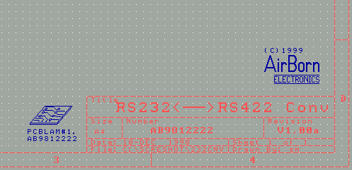
We create a new schematic diagram, allocating a name to the project, a version number to the schematic, and a drawing number for the printed circuit board. We also put on our copyright/logo, and a symbol that we use to record the PCB drawing number
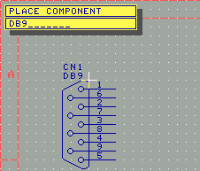
We place components on the schematic, for instance the DB9 connector through which the RS232 signals will be connected.
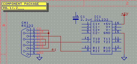
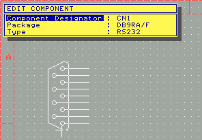 As we place the components, we edit the package details (and silkscreen legend 'Type') to match
what we want on the Printed Circuit Board.
As we place the components, we edit the package details (and silkscreen legend 'Type') to match
what we want on the Printed Circuit Board.
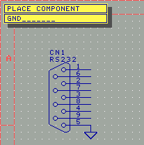 Items such as ground symbols, test points and jumpers are placed as different types of components.
The copyright/logo and PCB drawing number symbol (placed previously) were also different types of
components
Items such as ground symbols, test points and jumpers are placed as different types of components.
The copyright/logo and PCB drawing number symbol (placed previously) were also different types of
components
 Lines are placed to connect components, taking care to start the line exactly on the end of the
component pin.
Lines are placed to connect components, taking care to start the line exactly on the end of the
component pin.
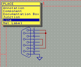
Lines can be inter-connected by placing junctions.
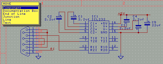
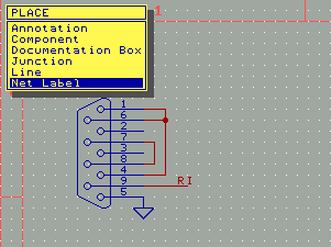 Signals that are not easily connected by lines may be connected by using a net label. A net label
(e.g. '+5V'; or 'RI' - ring indicator signal in the schematic below) will connect all points of
that name, even across multiple sheets if there is more than one sheet in the schematic.
Signals that are not easily connected by lines may be connected by using a net label. A net label
(e.g. '+5V'; or 'RI' - ring indicator signal in the schematic below) will connect all points of
that name, even across multiple sheets if there is more than one sheet in the schematic.
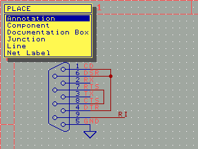 Annotation can be placed anywhere on a schematic, and it often helps to understand what signals
are on what pins. Depending on your CAD package, it may be easy to confuse Annotation and
Net labels - just remember that annotation is a note for the readers benefit - it does
not connect lines the way net labels do.
Annotation can be placed anywhere on a schematic, and it often helps to understand what signals
are on what pins. Depending on your CAD package, it may be easy to confuse Annotation and
Net labels - just remember that annotation is a note for the readers benefit - it does
not connect lines the way net labels do.
Reasonably extensive component libraries are available for most CAD packages. In any case,
check the components pinout against current data sheets. Where components are not in the library,
your CAD packages will allow you to define your own components, it is just a little extra work.
Some components have a choice of packages available, and it is important to consider the selection
carefully. Normally the component package type is selected at the schematic design stage, and
then carried through to the printed circuit board.
As the schematic progresses, text and components are ofcourse moved around to get a good circuit
layout.
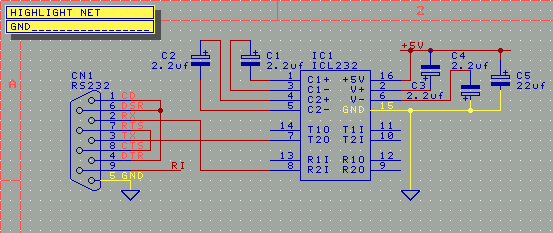
The net connection functions of the circuit diagram can be checked by the Highlight Net function
(may vary from package to package)
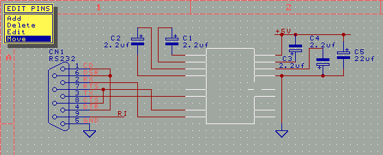
Existing library components can be edited (if required) to better fit the circuit diagram -
for instance by moving pins
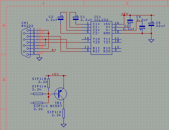
Some components have multiple parts - for instance individual resistors within a
Single-Inline-Package resistor network, or individual gates within a logic chip.
These may be indicated by a notation such as SIP1:B
A good schematic can show connectivity in addition to its main task of showing the functionality
of the circuit. This connectivity is part of the PCB layout task, but it is being thought through
at the schematic design stage.
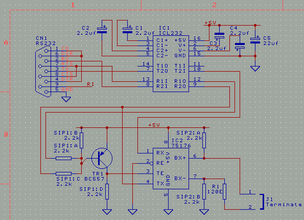
Resistor values are usually shown without the 'ohms' symbol - '2.2k' is a 2.2 kilo-ohm resistor,
120E is a 120 ohm resistor (other engineers may show this as 120R or just 120)
Schematics can be made more useful by descriptive labelling of connectors, option jumpers and
indicators. This labelling will then carry through to the Printed Circuit Board
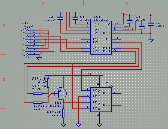
A power supply, power connector or batteries will be necessary for any project. The power supply
will also need decoupling capacitors.
When the schematic is complete, the project should be transferred to a Netlist for importing into the PCB CAD package. The details of this step are very dependent on the particular CAD packages you are using.
-------------------
C:\SCRESHOT>dir

 Volume in drive C has no label
 Volume Serial Number is 01B2-0295
 Directory of C:\SCRESHOT

.              [DIR]        12-10-98 12:16p .
..             [DIR]        12-10-98 12:16p ..
NOTES    TXT         4,244  12-11-98  2:44p notes.txt
232CNV   NET         1,765  12-11-98  2:53p 232CNV.NET
232CNV   S01        12,304  12-11-98  2:45p 232CNV.S01
ARCHIVE        [DIR]        12-10-98  3:47p ARCHIVE
232CNV   WIR         2,738  12-11-98  2:53p 232CNV.WIR
232CNV   REP           582  12-11-98  2:53p 232CNV.REP
232CNV   BOM         1,117  12-11-98  2:53p 232CNV.BOM
         6 file(s)         22,750 bytes
         3 dir(s)        4,172.28 MB free

C:\SCRESHOT>c:\schmatic\post 232cnv 232cnv
-------------------
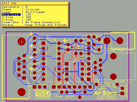
Before starting the Printed Circuit Board layout, the settings for the CAD package should be initialized. This is dependent on the type of circuit board you wish to produce, and the details are dependent on the type of CAD package that you use.
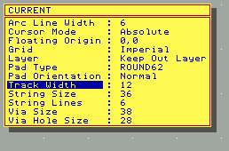
The example here shows the 'Current' settings. The board being designed will, in the main, use 12 thou tracks. A more simple loosely laid out circuit board might use 22 thou tracks. A more compact, tighter circuit board layout would normally use 8 thou tracks.
The via size being used has a hole diameter of 0.7mm (28 thou) and a quite small pad size of 38thou. Other designers might tend to use a pad size that is smaller again, because the smaller via sizes tend to make the design layout easier. However, small vias also make the PCB laminate manufacturing more expensive - the drills break more often and the yield goes down. For tight layouts, however, it would be worthwhile to use a smaller via pad and hole - typically a 16 thou hole (0.4mm) and a 28 thou pad. In this project, small vias just aren't needed, the layout is simple enough with the medium size vias.
If you are using the CAD package we have shown in our example, make sure all your string sizes are in multiples of 12 thou - e.g., 36, 48 or 60 thou - as there is a bug in the package that rounds to this value
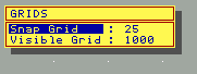
An imperial grid at 25 thou is usually the best coordinate system for standard, relaxed printed circuit board designs such as this one. As the density increases, designers usually drop to a 5 thou grid. Some designers use gridless routing, but it never looks as nice, and you get a whole load of "intangible benefits" from gridded routing - you can be reasonably confident about clearances, vias often happen to be in the right position for extra component leads - that sort of thing.
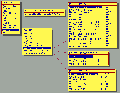
Again, Depending on your CAD package, there will be setup required in other areas involved with Netlists and Routing. To some degree, these options depend on how you will use the CAD package. In the particular package we are showing as an example we would not use the autorouter for more than checking completion progress - hence the options set.
You will also have to ensure the components to be used in the PCB are available in the CAD parts Library.
If you use the CAD package shown in the example, you should be aware that there is a limit on how many components may be in a library. You may either produce a library for each individual project (which you may find quite tedious) or you may load each library in turn, and run the 'N-A-L' keyboard command sequence (Netlist-Autoplace-LoadfromNet) on each library to load the components used in that library. This also allows you the opportunity to have more libraries, you can always sign up for ours: AirBorn Electronics Autotrax Library
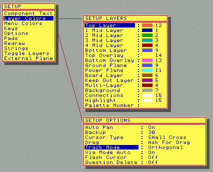
There will also be options to setup personal preferences such as colours.
Loading the netlist will be very dependent on the particular CAD package you are using.
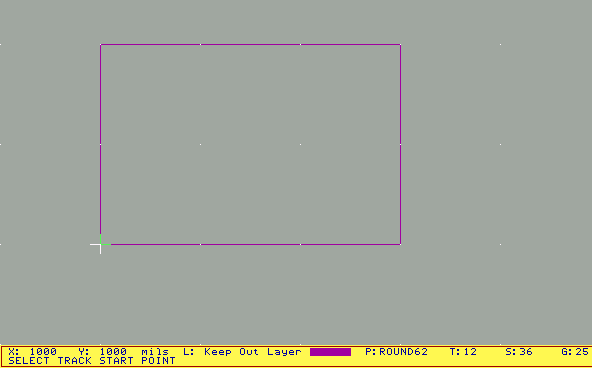
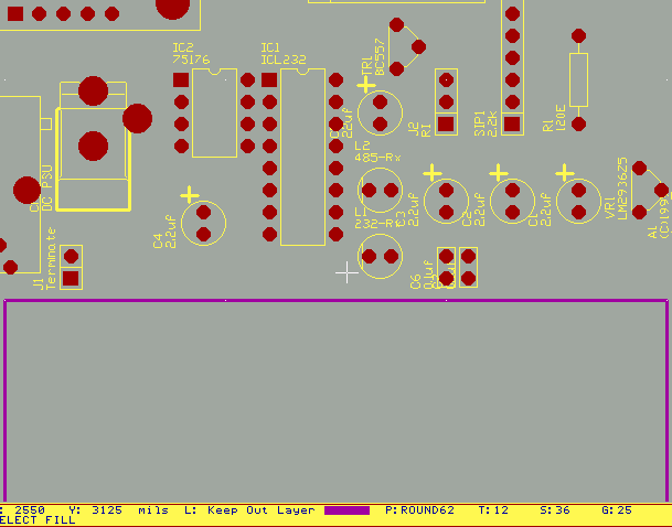
In our example CAD package, the first step is to place a basic border on the keep out layer.
In our example we took a guess at 2 inches by 3 inches - we can change it later.
Remember to save your work frequently as you proceed through the next stages if you are
following our example.
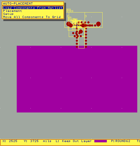
For our example we place a 'Fill' on the keepout layer, covering the
whole of the circuit board. Then we do the 'N-A-L' keyboard sequence
(Netlist-Autoplace-LoadfromNet) to load the components. The components
are pulled from the library and piled in a heap at the cursor position -
we put them above the circuit board.
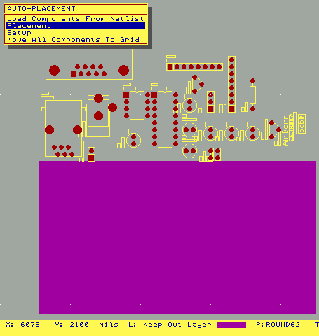
After executing the 'N-A-L' sequence to load the parts from the library
on to the board, we proceed to a 'N-A-P' (Netlist-Autoplace-Placement)
to spread the components out so we can see them easily. These two operations
only take a couple of seconds - just a few keystrokes, the package does the work
After executing the 'N-A-P' sequence we delete the fill that we had
covering the circuit board. We now have all the components read in,
and we can begin to place them. If there were any problems we would
have encountered an error message, and the details would have been
written to a .REP (report) file
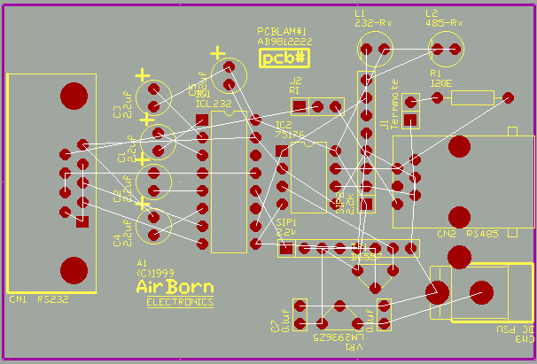
While placing the components, we can view the connections to be made
using the 'N-S-A' (Netlist-Show-All) keyboard sequence. This can be
used as a guide to achieve a starting layout
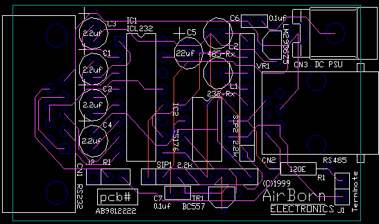
Naturally some reorganisation goes on until a good layout is achieved
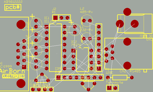
After a good layout has been achieved, usually the border will be
moved in to get a smaller board size. The labels will be moved
around so that a good legend can be printed on the PCB
Designers will frequently autoroute part of a Printed Circuit Board
layout. Even the best autorouters require a great deal of supervision
and certainly some amount of cleaning up afterwards. And then there
are some autorouters that are just plain shoddy and shouldn't be used:
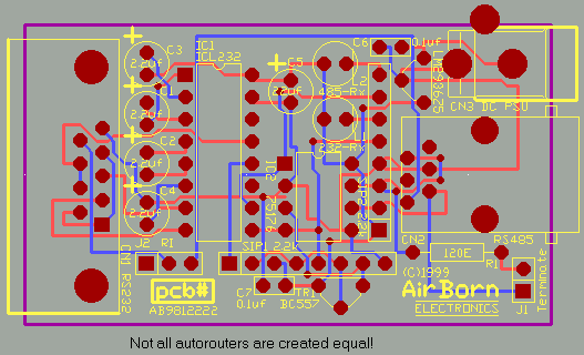
There are some areas of any circuit design that really should not be
autorouted. There are some designs where none of the circuitry, at all,
should be autorouted. The attraction of autorouters is that they save
design time, it is very tempting to hit "Go" and to think you can have
your board finished shortly afterwards, with no effort at all.
Beware any company that tells you their router is atleast as good as manual placement by a design engineer - remember those same software vendors also force you to waive statutory rights and most warranties before you open the shrinkwrap!
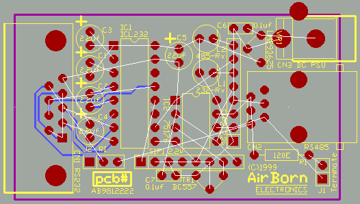
Manual routing uses the netlist as a guide. Manual routing can take
intelligent advantage of contours, weighing complex decisions about
track currents, noise pickup and grounding loops to achieve the best
pattern. Tracks usually run on both sides of the printed circuit
board (tracks on the solder side of the board are seen here in blue)
however, some boards are simpler single sided, and other boards are
more complex multilayer boards - most with four layers, but some
with six or more layers
Layers can be switched on and off in the CAD package so that it is
easier to see the tracks that are being routed. As we mentioned
before, our example is mostly going to use 12 thou tracks - most of
our PCB is spaced '12 by 12' ie 12 thou tracks and 12 thou clearance
between tracks/tracks and tracks/pads. Another way of referring to
the tolerance is 12 thou tracks on a 25 thou spacing (the grid size)
Heavier tracks are usually used for Power and Ground connections,
in order to allow for the heavier current flow and to reduce
impedance of the connections. Higher current connections (not
applicable to this design) need tracks with calculated widths.
Ground is usually the most important connection in a PCB layout. While it is difficult to describe all the rules, as they tend to interact and vary somewhat from design to design, the basic idea is to achieve a low impedance ground and minimize undesirable interaction between circuitry that can result from excessive current flow through the ground connections - especially under fault conditions.
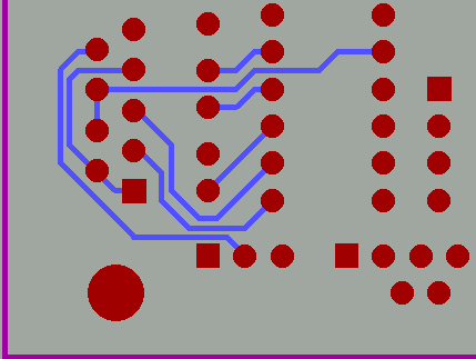
The routes that were made visible using the 'Netlist-Show-All'
command sequence are a guide to completing the PCB layout. By
using the autorouter to only 'Process Pre-routes' instead of
routing, we are able to eliminate the nets that have been placed
as tracks already. As a result only those nets still to be placed
are visible
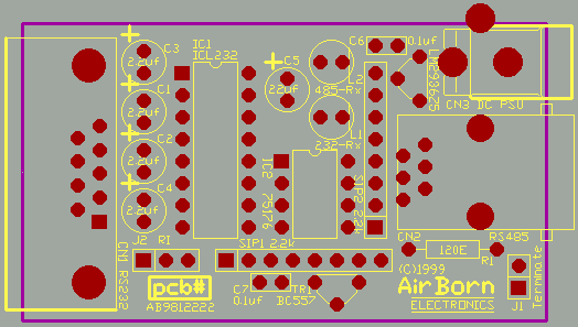
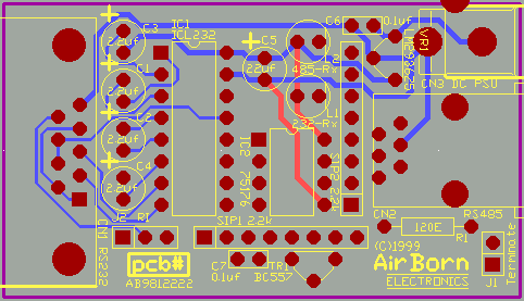
When the board is complete, no more routes are visible. At this
stage a Design Rule Check operation can be performed, this will
test the PCB layout against the netlist and a set of rules
previously specified. Any violations encountered will be reported
(e.g. in a .DRC log file).
In a larger PCB design, there might be several iterations between schematic and PCB. For instance, it might be more convenient for layout to swop different gates (or SIP resistor) in a package, rather than use the one specified in the circuit. In the example CAD package shown, it is necessary to go back into the schematic package, edit the schematic, regenerate the netlist (using POST), and then re-import the netlist into the PCB CAD package. While this sounds arduous, it is quite easy to have all 3 programs running simultaneously under windows, and simply 'Alt-Tab' between them, so the modification is accomplished reasonably easily. Other CAD packages have 'back annotation' that accomplishes this task automatically.
Once the PCB has been completed and checked, a Bill-Of-Materials can be generated from it. In the case of the example CAD package, this is done by using the BOM.EXE utility.
-------------------------------------------------------------------------------
232CNV.PCB  21:14  11-12-1998    Bill of Material Detail    Page : 1
-------------------------------------------------------------------------------
DESIGNATOR         COMMENT                             PATTERN

A1                 (C)1999                             AIRBORN
C1                 2.2UF                               RB.1/.2
C2                 2.2UF                               RB.1/.2
C3                 2.2UF                               RB.1/.2
C4                 2.2UF                               RB.1/.2
C5                 22UF                                RB.1/.2
C6                 0.1UF                               RAD0.1
C7                 0.1UF                               RAD0.1
CN1                RS232                               DB9RA/F
CN2                RS485                               RJ12
CN3                DC PSU                              DCSKT2.5
IC1                ICL232                              DIP16
IC2                75176                               DIP8
J1                 TERMINATE                           SIP2
J2                 RI                                  SIP3
L1                 232-RX                              LED5
L2                 485-RX                              LED5
PCBLAM#1           AB9812222                           PCLAMINATE
R1                 120E                                AXIAL0.4
SIP1               2.2K                                SIP8
SIP2               2.2K                                SIP8
TR1                BC557                               TO-92A
VR1                LM2936Z5                            TO-92A

Total Components = 23
---------------------
You can see that our PCLAMINATE component has carried through from the original schematic, through the Printed Circuit Board, into the Bill-Of-Materials. By using a unique number for each issue of PCB, we can tie all three items together with this component. Our copyright/logo has also appeared in all three files, using the same method.
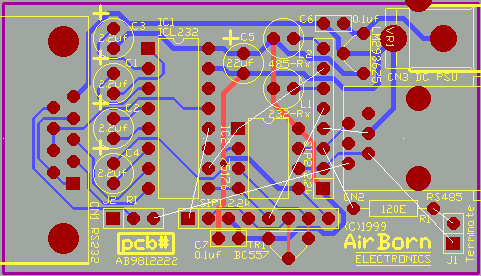
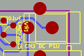 Our PCB still requires a little bit of cleaning up, as there is
a pad overlapping the side of the PCB. While silkscreen legend
can overlap the side of a PCB - it doesn't usually cause any
problems - holes over the edge of the PCB will usually interfere
with the routing or V-Grooving of the board.
Our PCB still requires a little bit of cleaning up, as there is
a pad overlapping the side of the PCB. While silkscreen legend
can overlap the side of a PCB - it doesn't usually cause any
problems - holes over the edge of the PCB will usually interfere
with the routing or V-Grooving of the board.
So we should fix this...
Next we check hole sizes of Pads on the PCB. The hole size required varies with the particular type of component. Incorrect hole size is a major source of error in producing PCBs.
If we have a manufacturer producing an enclosure for our electronic device, we can export an Autocad format mechanical file using the PCBTODXF.EXE utility.
Refer to our documentation page to see the total package that we
put together for the Printed circuit board. The SCHPLOT.EXE utility
is used to print the schematic diagram. The PLOT.EXE utility is
used, with appropriate options selected, to print the checkplot
(actual size and or enlarged as required) and the drilling diagram.
As described above we use the BOM.EXE utility to print the parts
list from the PCB itself, although we massage the result slightly
using a program of our own called BOM2PART.EXE, to reorder the
parts list by item (this was not necessary for our example PCB).
We add an ECO notes sheet, a parts list key, and a front cover,
and then the documentation file for the Printed Circuit Board is
complete.
Most CAD packages finish the job by saving the file as either native format, or preferably Gerber, to be sent to the PCB manufacturer to have the boards produced.
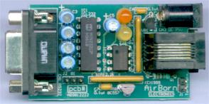
The prototype board is assembled and tested, and, we find a fault.
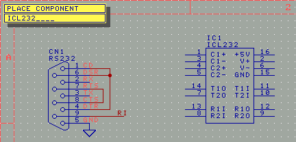
We have connected the Rx input on the D9 to the Rx input of the IC232, and the Tx output on the D9 to the Tx output of the ICL232. It won't work. The Rx input on the D9 is the Rx input of the device it is connected to - for instance a PC - and it needs to be connected to the Tx output of the ICL232. This is actually a common mistake.
Frankly, we do find it helpful to quietly go back try and work out how such mistakes happened. Sometimes we can modify systems to prevent them happening again. Unfortunately for us in this project, the original prototype and paper notes were trashed as we moved premises shortly after the job was completed. In any case, suddenly we have a very realistic tutorial - this is why prototypes get built, so that mistakes can be found.
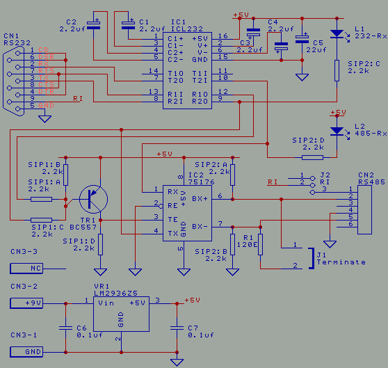
So we fix the circuit by connecting the CN1 D9 PC Rx input (pin 2) to Pin 7 T20 of ICL232, and
CN1 D9 PC Tx output (pin 3) to Pin 8 R2I of ICL232. We also update the version number of
the schematic to V1.10, to indicate the changed circuit, and the drawing number symbol to
AB09906847 to indicate the new schematic/pcb/parts list revision, that way we can keep
track of which boards have the error, and which do not
(See Eco and Version Numbers).
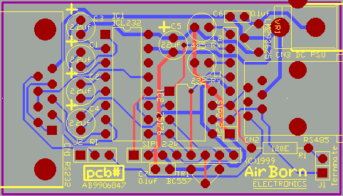
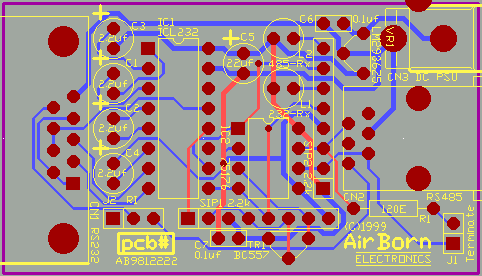
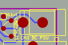
The fixed PCB
©2013 AirBorn - Last updated 01 May 2013