
2 Wire Input/Output for 8051 type CPU's
|
This article was written in 1996. While the principles are still quite valid, the landscape has changed.
Todays CPUs come with an SPI port, (SPICLK = SCLK), and it just can be easier to use this
than to build your own. With SPI the data lines are seperate (MOSI = SOUT and MISO= SIN).
You still need to arrange for an SSTB, perhaps by using the SPI SS line. With many CPUs the
polarity of the Clk and edge is programmable to suit your devices. Also, in addition to the logic
shift registers shown here there are now many other specialist SPI devices on the market.
|
When using single chip micro's, especially the smaller single chip micro's like the AT89C2051, it is often desirable to expand the I/O serially.
One good method of serial expansion, practised widely, is the use of the i2c bus. The i2c bus is versatile, and needs only two wires for communication, but unfortunately the parts are a little expensive. If you need the versatility of being able to add not only parallel I/O, but devices like EEPROM, RAM and clocks, then the i2c bus is for you, and you should refer to the excellent application note from Atmel, or the full information from Philips, concerning this approach.
Sometimes cost and simplicity are more important than versatility. The simplest form of I/O expansion uses shift registers. To put this in dollar terms, the (total) cost of implementing an 8 bit I/O port in i2c technology is around the $3 mark, while in shift register logic it is around 0.75c. Also, if required, 4094 shift register outputs can be tri-stated at power up until the CPU has written valid data, preventing power up "glitches"

Normally four I/O lines are needed
- Serial clock (Signal to clock data in/out of the shift registers)
- Serial data out (Data out to the shift registers)
- Serial data in (Data in from the shift registers)
- Serial strobe (Signal to load data into the shift registers)
Shift registers can be cascaded as required, and the software to input and output is quite simple. Four I/O pins can be a lot to lose, however. For the cost of a few passive components the arrangement shown implements 2 wire I/O for an 8051 using shift registers.
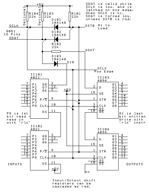
The circuit as shown requires that the software access be performed in a certain way
2 Wire Serial IO Driver software requirements
- The inputs are read in first, one bit at a time
- Send SCLK low
- Write 1 to SDAT - it will stay low if the input data is 0
- After a brief settling delay, SDAT is read
- The first bit read is P8, so bit input should be done using the "rlc" instruction
- Send SDAT low
- Send SCLK high (simultaneously with SDAT low, if possible)
- The process repeats until all the input bits are read (8,16, 24 or 32 of them)
- The outputs are written out, one bit at a time
- Send SCLK low
- SDAT is written with the data to be output (simultaneously with SCLK lo, if possible)
- The last bit output is Q1, so bit output should be done using the "rlc" instruction
- After a brief settling delay, Send SDAT low
- SCLK must be asserted high simultaneously with SDAT being asserted low
- (The simultaneous operation is achieved using "mov px,acc" instruction)
- (The CD4094 will latch the data present on SDAT before the SCLK transition)
- The process repeats until all the output bits are written (8,16,24 or 32 of them)
- Now the inputs have been read, and outputs written, the strobe is sent.
- SCLK should still be high, as this is its default state
- Send SDAT high.
- A settling delay is allowed - a few machine cycles
- As both SDAT and SCLK are high, SSTB goes high
- SSTB going high loads the data shifted to the output shift registers to the output lines
- SSTB going high also loads the input shift registers with the current input data
- Send SDAT low, sending SSTB low again
- The input/output cycle is now complete, and a new one can start when required
 The first set of inputs read after reset will not be correct, as no strobe pulse was generated to load the registers, however they must be read, as otherwise it is not possible to load the outputs with valid data. The outputs can be held in the "off" state after reset by controlling them with the OE line on the CD4094, if desired. While the OE lines to the CD4094's are held low, the outputs will be tristate. So at reset, the procedure should be to do a dummy read of all the inputs, then start normal output/input cycles, and enable the outputs by setting the OE line of the CD4094's high.
For explanation purposes, it was necessary to show the driver software above doing input, output, then strobe. However, for implementation purposes, it may be more desirable to do the software as output, strobe, then input. As long as the dummy inputs are done at power up, this is the same operation stated a different way. The advantage of performing the operation as output, strobe, input, is that the latest input values are read, no matter how long ago the last I/O operation occurred.
 Contact Info Contact Info
 Home Home
 Overview Overview
 Continue Continue
 Bye Bye
Written 1996, Updated ©2010 AirBorn
|