 
HSETI1 PCB: An 89C2051 CPU, 8 driver outputs (e.g. LEDs, relays), a speaker output, a light sensor input, 3 extra inputs, optional serial port, small simple PCB.
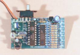
This document describes the HSETI PCB. This PCB is a small simple application for the Atmel AT89C2051 microprocessor - a 20 pin 8051 variant, with FLASH (reprogrammable) program memory. The board has just two chips on it, the CPU and a driver/buffer.
Contents of this project - all downloadable
- PCB diagram
- Circuit diagram, B/W image, download and print
- Circuit description
- Circuit diagram, protel CAD format
- PCB art, overlay, 300dpi .GIF
- PCB art, top layer, 300dpi .GIF - for make your own PCBs
- PCB art, bottom layer, 300dpi .GIF - for make your own PCBs
- PCB art, drilling diagram
- PCB layout, protel CAD format
- Parts list
- Parts Description
- Parts notes
- Programming the HSETI PCB
- Program code, 8051 assembler, well commented
- tasm32.zip (or original from telemark) -Assembler tools to compile the program code
- Typical connection circuit for HSETI PCB
Other Projects: Library
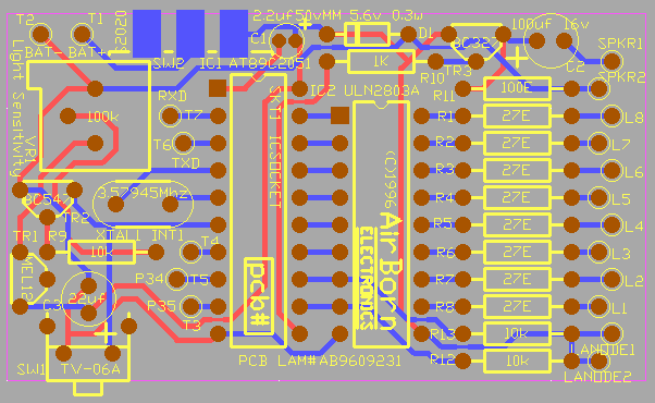
The PCB diagram is pictured above. Central to the board are the two ICs: The AT89C2051 (in an IC socket) and ULN2803 driver. The bank of resistors to the right of the ULN2803 are primarily for limiting the current through LEDs, when they are being driven direct from the outputs. You may wish to use another value instead of the 27 ohm shown on the circuit. The circuitry to the left of the CPU is primarily for the light sensor - this is just a simple darlington phototransistor, sensitivity pot and switch transistor.
Circuit diagram
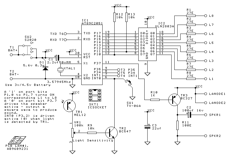 The circuit diagram is pictured above.
- This is a very simple application of a single chip microprocessor (IC1).
- The battery power supply is connected on terminals T1 &T2. While the circuit diagram specifies 3v/4.5v battery, the part ULN2803 needs 4.5v-5v battery to get proper operation.
- Switch SW2 allows the PCB to be turned on and off.
- Capacitor C1 provides a reset signal to the microprocessor.
- XTAL1 provides the oscillator timing component for the microprocessor. It is important to use a crystal for XTAL1, not a ceramic resonator - prototype testing shows that a ceramic resonator gives problems unless capacitors to ground are placed on X1 & X2.
- Diode D1 provides some protection for the microprocessor in case of transients or mis-connection of the battery
- Optodarlington TR1 is the light sensor
- Pot VR1, as labelled, adjusts the sensitivity of the light sensor
- Resistor R9 provides current limiting when full illumination is on TR1 at max sensitivity
- TR2 is a switch used to sense illumination (On=TR1 illuminated)
- Pin 6 of the micro is the LiteOn input (Low=TR1 illuminated)
- SW1 is in parallel with the LiteOn input - pushing SW1 is like illuminating TR1
- Resistors R12 & R13 pull up the open collector outputs P1.0 and P1.1 of IC1
- IC2 is the driver IC, with several hundred milliamps drive capability on each output
- R1-R8 limit the current that can be taken from each output of IC2, and are most useful when LEDs are connected directly to pins L1-L8. If other devices are used, such as relays, the values may of R1-R8 may have to be changed, or replaced with links.

- R10 limits the current from IC1 into the base of TR3
- TR3 is a switch transistor that drives the sounder output (P3.7 Low=Sounder driven high)
- R11 provides the class A load resistor for the sounder output
- C2 Capacitively couples the speaker to TR3 and R11.
- C3 provides some supply decoupling.
- The symbol PCB LAM#1 is a record of the PCB laminate ID number, and ensures the PCB laminate appears in the parts list
- The symbol SKT1 is a record of the need for a socket for IC1, and ensures that the socket appears in the parts list
HSETI Schematic - Protel format CAD file
The HSETI schematic, in protel CAD format, can be obtained through the above link.
To continue on and see the rest of the PCB diagrams, the parts list and wiring, use the 'continue'
link below.
 Continue - PCB Diagrams Continue - PCB Diagrams
|